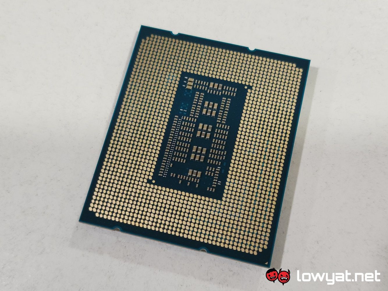
For another matter, Intel also made it clear that it intends to keep Moore’s Law alive – it was also the 75th anniversary of the technology – and to that end, it is now aiming on having a package so dense, it would house up to one trillion transistors by 2030.
“Seventy-five years since the invention of the transistor, innovation driving Moore’s Law continues to address the world’s exponentially increasing demand for computing. At IEDM 2022, Intel is showcasing both the forward-thinking and concrete research advancements needed to break through current and future barriers, deliver to this insatiable demand, and keep Moore’s Law alive and well for years to come.” Gary Patton, vice president and general manager of Components Research and Design Enablement at Intel, said. As to the how of reaching one trillion transistors, it all goes back to the earlier mentioned 10x interconnect density; this begins with the introduction of what the chipmaker calls quasi-monolithic chips, using a continued hybrid bonding scaling to a 3um pitch. Additionally, the company is also looking at super-thin “2D” gate-all-around stacked nanosheets that are just three atoms thick, which should pave the way towards it developing high-performing and scalable transistor channels. “Continuous innovation is the cornerstone of Moore’s Law. Many of the key innovation milestones for continued power, performance and cost improvements over the past two decades – including strained silicon, Hi-K metal gate and FinFET – in personal computers, graphics processors and data centres started with Intel’s Components Research Group. Further research, including RibbonFET gate-all-around (GAA) transistors, PowerVia back side power delivery technology and packaging breakthroughs like EMIB and Foveros Direct, are on the roadmap today,” said Intel in its official press statement. (Source: Intel)

