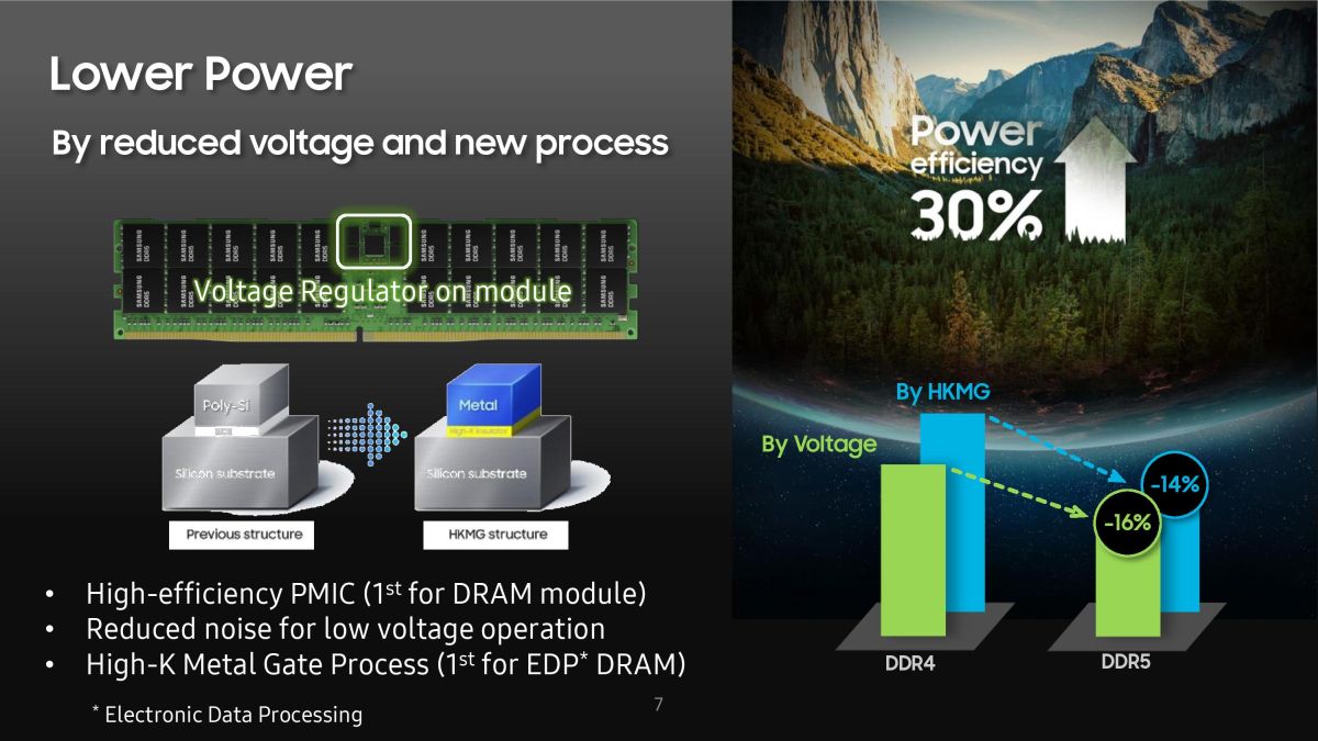
According to the multiple reports, the new memory module will follow the current DDR5 specifications standards; the modules will run at the lower 1.1V, along with JEDEC DDR5-7200 CL timings. That said, it should be pointed out that even JEDEC itself has not announced any timing for the memory modules, at least officially anyway. At most, the body has only released such information for DDR5-6400 modules. Moving on, Samsung’s presentation also showed that the new DDR5-7200 module will be the first memory module to use the Same-Bank refresh (SBR) technology that is designed to increase the efficiency of the DRAM bus connectivity by approximately 10%. Additionally, the memory module will also introduce Decision Feedback Equaliser (DFE).
As for how Samsung managed to create memory modules with such a humongous capacity, the technology giants says that each module comprises eight dies, stacked together and yet, is still significantly smaller than the current four-die stack on DDR4 memory modules. The process is known as through-silicon-via topographies, and by its account, reduces the gap between dies by around 40%. As for when the new DDR5-7200 RAM will be ready, Samsung expects its new ram module to enter mass production nearing the end of the year, meaning that availability could be as early as the start of next year. (Source: AnandTech)
